- 您现在的位置:买卖IC网 > Sheet目录312 > AT26DF161-SU (Atmel)IC FLASH 16MBIT 66MHZ 8SOIC
�� �
�
�The� AT26DF161� also� offers� a� sophisticated� method� for� protecting� individual� sectors� against�
�erroneous� or� malicious� program� and� erase� operations.� By� providing� the� ability� to� individually� pro-�
�tect� and� unprotect� sectors,� a� system� can� unprotect� a� specific� sector� to� modify� its� contents� while�
�keeping� the� remaining� sectors� of� the� memory� array� securely� protected.� This� is� useful� in� applica-�
�tions� where� program� code� is� patched� or� updated� on� a� subroutine� or� module� basis,� or� in�
�applications� where� data� storage� segments� need� to� be� modified� without� running� the� risk� of� errant�
�modifications� to� the� program� code� segments.� In� addition� to� individual� sector� protection� capabili-�
�ties,� the� AT26DF161� incorporates� Global� Protect� and� Global� Unprotect� features� that� allow� the�
�entire� memory� array� to� be� either� protected� or� unprotected� all� at� once.� This� reduces� overhead�
�during� the� manufacturing� process� since� sectors� do� not� have� to� be� unprotected� one-by-one� prior�
�to� initial� programming.�
�Specifically� designed� for� use� in� 3-volt� systems,� the� AT26DF161� supports� read,� program,� and�
�erase� operations� with� a� supply� voltage� range� of� 2.7V� to� 3.6V.� No� separate� voltage� is� required� for�
�programming� and� erasing.�
�2.� Pin� Descriptions� and� Pinouts�
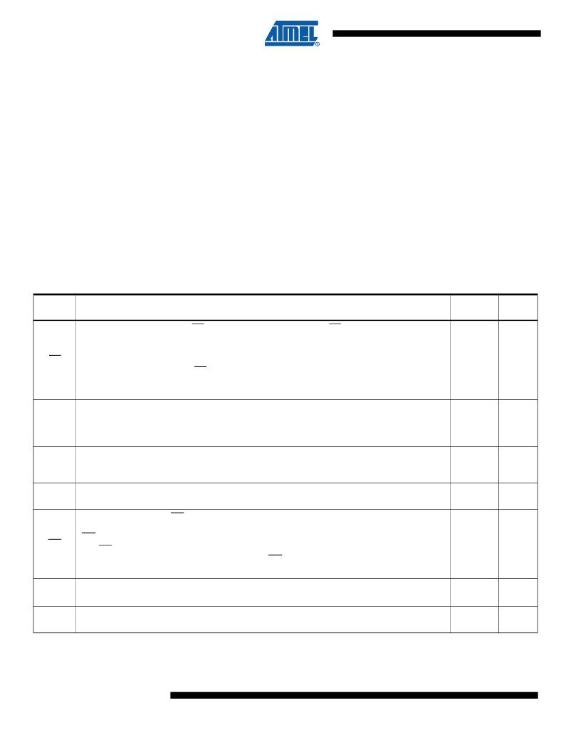
�Table� 2-1.�
�Pin� Descriptions�
�Asserted�
�Symbol�
�Name� and� Function�
�State�
�Type�
�CHIP� SELECT� :� Asserting� the� CS� pin� selects� the� device.� When� the� CS� pin� is� deasserted,� the�
�device� will� be� deselected� and� normally� be� placed� in� standby� mode� (not� Deep� Power-Down� mode),�
�and� the� SO� pin� will� be� in� a� high-impedance� state.� When� the� device� is� deselected,� data� will� not� be�
�CS�
�accepted� on� the� SI� pin.�
�Low�
�Input�
�A� high-to-low� transition� on� the� CS� pin� is� required� to� start� an� operation,� and� a� low-to-high� transition�
�is� required� to� end� an� operation.� When� ending� an� internally� self-timed� operation� such� as� a� program�
�or� erase� cycle,� the� device� will� not� enter� the� standby� mode� until� the� completion� of� the� operation.�
�SERIAL� CLOCK� :� This� pin� is� used� to� provide� a� clock� to� the� device� and� is� used� to� control� the� flow� of�
�SCK�
�SI�
�SO�
�data� to� and� from� the� device.� Command,� address,� and� input� data� present� on� the� SI� pin� is� always�
�latched� on� the� rising� edge� of� SCK,� while� output� data� on� the� SO� pin� is� always� clocked� out� on� the�
�falling� edge� of� SCK.�
�SERIAL� INPUT� :� The� SI� pin� is� used� to� shift� data� into� the� device.� The� SI� pin� is� used� for� all� data� input�
�including� command� and� address� sequences.� Data� on� the� SI� pin� is� always� latched� on� the� rising�
�edge� of� SCK.�
�SERIAL� OUTPUT� :� The� SO� pin� is� used� to� shift� data� out� from� the� device.� Data� on� the� SO� pin� is�
�always� clocked� out� on� the� falling� edge� of� SCK.�
�WRITE� PROTECT� :� The� WP� pin� controls� the� hardware� locking� feature� of� the� device.� Please� refer� to�
�“Protection� Commands� and� Features”� on� page� 11� for� more� details� on� protection� features� and� the�
�Input�
�Input�
�Output�
�WP�
�WP� pin.�
�The� WP� pin� is� internally� pulled-high� and� may� be� left� floating� if� hardware� controlled� protection� will�
�Low�
�Input�
�not� be� used.� However,� it� is� recommended� that� the� WP� pin� also� be� externally� connected� to� V� CC�
�whenever� possible.�
�2�
�V� CC�
�GND�
�DEVICE� POWER� SUPPLY� :� The� V� CC� pin� is� used� to� supply� the� source� voltage� to� the� device.�
�Operations� at� invalid� V� CC� voltages� may� produce� spurious� results� and� should� not� be� attempted.�
�GROUND� :� The� ground� reference� for� the� power� supply.� GND� should� be� connected� to� the� system�
�ground.�
�AT26DF161�
�Power�
�Power�
�3599H–DFLASH–8/09�
�发布紧急采购,3分钟左右您将得到回复。
相关PDF资料
AT26DF161A-MU
IC FLASH 16MBIT 70MHZ 8QFN
AT26DF321-SU
IC FLASH 32MBIT 66MHZ 8SOIC
AT27BV010-90JU
IC OTP 1MBIT 90NS 32PLCC
AT27BV020-90JU
IC OTP 2MBIT 90NS 32PLCC
AT27BV040-12JU
IC OTP 4MBIT 120NS 32PLCC
AT27BV1024-90JU
IC OTP 1MBIT 90NS 44PLCC
AT27BV256-70JU
IC OTP 256KBIT 70NS 32PLCC
AT27BV4096-12VI
IC OTP 4MBIT 120NS 40VSOP
相关代理商/技术参数
AT26DF321
制造商:ATMEL 制造商全称:ATMEL Corporation 功能描述:32-megabit 2.7-volt Only Serial Firmware DataFlash Memory
AT26DF321_06
制造商:ATMEL 制造商全称:ATMEL Corporation 功能描述:32-megabit 2.7-volt Only Serial Firmware DataFlash Memory
AT26DF321_07
制造商:ATMEL 制造商全称:ATMEL Corporation 功能描述:32-megabit 2.7-volt Only Serial Firmware DataFlash Memory
AT26DF321-S3U
功能描述:闪存 32M SERIAL FLASH - IND TEMP RoHS:否 制造商:ON Semiconductor 数据总线宽度:1 bit 存储类型:Flash 存储容量:2 MB 结构:256 K x 8 定时类型: 接口类型:SPI 访问时间: 电源电压-最大:3.6 V 电源电压-最小:2.3 V 最大工作电流:15 mA 工作温度:- 40 C to + 85 C 安装风格:SMD/SMT 封装 / 箱体: 封装:Reel
AT26DF321-SU
功能描述:闪存 32M SERIAL FLASH - IND TEMP RoHS:否 制造商:ON Semiconductor 数据总线宽度:1 bit 存储类型:Flash 存储容量:2 MB 结构:256 K x 8 定时类型: 接口类型:SPI 访问时间: 电源电压-最大:3.6 V 电源电压-最小:2.3 V 最大工作电流:15 mA 工作温度:- 40 C to + 85 C 安装风格:SMD/SMT 封装 / 箱体: 封装:Reel
AT26DF321-SU SL514
制造商:Atmel Corporation 功能描述:
AT26F004
制造商:ATMEL 制造商全称:ATMEL Corporation 功能描述:4-megabit 2.7-volt Only Serial Firmware DataFlash Memory
AT26F004_06
制造商:ATMEL 制造商全称:ATMEL Corporation 功能描述:4-megabit 2.7-volt Only Serial Firmware DataFlash Memory